

Since high-speed communication is inevitable for evolving wireless systems, the demand for a higher data rate, higher frequency, larger spectrum, and wider bandwidth increases. When dealing with a wide bandwidth, multiple devices may have to be deployed in a wireless communication system to filter out unwanted noise and interfering signals, enhance the signal-to-noise ratio, and improve the sensitivity. A single tunable filter can replace these devices, reducing the system’s size and weight and the fabrication cost of multiple components.
Modeling a Tunable Cavity Filter with a Piezoelectric Actuator
Tunable devices can be realized using varactors, phase shifters, or switches with which the reactance, phase, or path of the signal can be tweaked and the frequency response of the device is changeable. Here, a tunable bandpass filter model is designed with a piezoelectric actuator that controls the reactance of the device and results in a variable resonance frequency of the filter.
The filter design is based on a rectangular cavity filter whose resonance frequencies are given by:
where a and b are the waveguide aperture dimensions and d is the length of the waveguide cavity.
The cavity width, height, and length are a = 100 mm, b = 50 mm, and d = 50 mm, respectively, to generate 3.354 GHz of the resonance frequency for the TE101 dominant mode.
Inside the cavity, a metallic post is added and configured to create a gap between the top surface of the post and ceiling of the cavity, so the height of the post is slightly smaller than b. When the cavity is resonant at the dominant mode, the energy is confined in the center of the cavity and the response of the gap that is located in the middle becomes capacitive. The extra capacitance lowers the resonance frequency by keeping the same structure size, so the device size is effectively reduced as well.
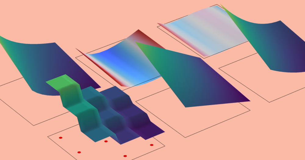
Two shorted 50-Ω microstrip lines, which are terminated by lumped ports, are coupled into the cavity through slots on the top of the cavity. Input matching (S11) and insertion loss (S21) can be improved by adjusting the dimensions and locations of the slots. A circular aperture at the top of the cavity is closed with a piezoelectric actuator, and the bottom surface of the disk is finished with a layer of a material where the conductivity is high enough to have a very small skin depth.
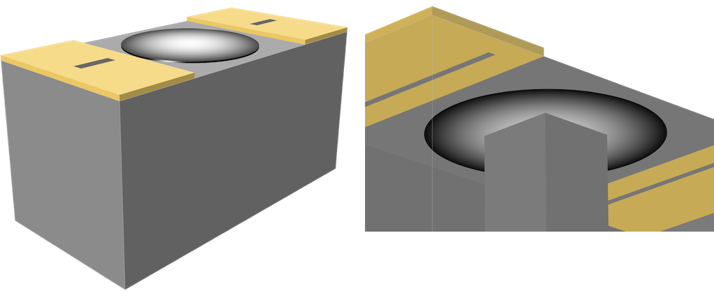
Left: The cavity filter with a piezoelectric actuator shaped like a circular disk. The feed scheme is built with slot-coupled microstrip lines. Right: The gap size between the piezoelectric actuator and metallic post controls the resonance frequency.
All metal parts — e.g., the cavity walls, post, substrate ground planes, microstrip lines, and bottom surface of the piezoelectric device — are set as perfect electric conductors (PECs). Lead zirconate titanate (PZT-5H) is used for the piezoelectric actuator. The actuator is z-polarized, resulting in mainly z-directional deflection of the device.
When a positive DC bias is applied across the piezoelectric actuator, it will deflect toward the bottom of the cavity. This deflection makes the capacitance stronger and shifts the resonance frequency lower than the case without any deformation. The animation below plots the electric field norm at the resonance frequency. At the center of the cavity, as well as in the gap between the top of the post and the bottom of the piezo device, strong electric fields are observed.
Accurately Analyzing an RF Filter with Multiphysics Simulation
The conventional analysis method for this type of device is using a parametric sweep of the height of the metallic post geometry (instead of warping the piezoelectric actuator parabolically) to see the change of the capacitance of the filter. However, in reality, the metallic post is fixed and the actual deformation of the piezoelectric actuator is not geometrically uniform. For this reason, the parametric sweep does not address the capacitance change precisely; thus, the evaluated resonance frequency is not accurate.
To describe the real-world phenomena, the elastic deformation of the actuator and the resulting capacitance change have to be modeled with a multiphysics approach that combines a high-frequency electromagnetic and piezostructural analysis. Using this approach is seamless and intuitive in the COMSOL Multiphysics® software, as it offers you a single simulation platform.
The multiphysics and moving mesh settings in a single simulation platform to model the deformation of the piezoelectric actuator.
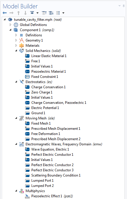
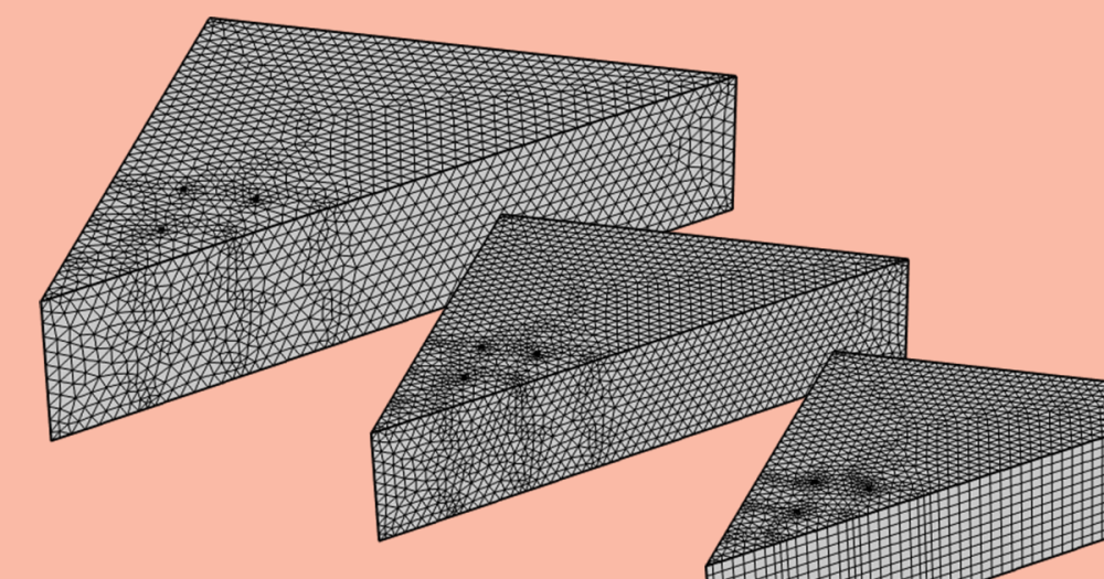
The deformation of the piezoelectric actuator is addressed via the combination of a few physics interfaces: the Solid Mechanics (solid), Electrostatics (es), and Moving Mesh (ale) interfaces. When the piezoelectric device deforms due to a positive and negative DC bias, the Moving Mesh interface is used to reconfigure the mesh for the Electromagnetic Waves, Frequency Domain interface, which calculates the wave propagation and resonance behavior in the microstrip lines and cavity.
By changing the resonance frequency, the electric field around 3 GHz is evanescent. The deformation of the piezoelectric actuator is exaggerated for visualization purposes. A surface plot of the electric field norm and an arrow plot of the electric field are also shown in the animation.
With an electric potential of +300 V across the piezoelectric actuator, a deflection of ~90 μm is observed, making the gap smaller and the capacitance in the gap stronger. Thus, the shift of the resonance frequency is lower than the shift at 0 bias as well as at negative bias.
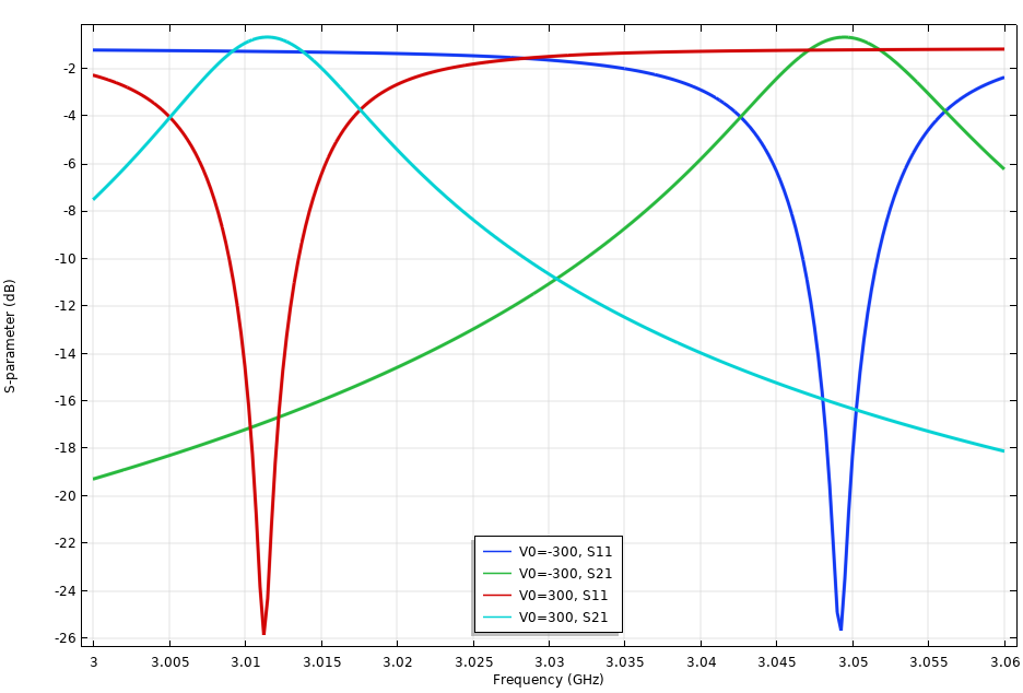
The S-parameters of the tunable cavity filter. The mode uses a DC bias of ±300 V.
The S-parameter plot shows the effect of the piezoelectric device deflection on the filter’s resonance frequency. The tunable frequency range of this example is around 40 MHz. This range can be adjusted by different choices of the piezoelectric disk size and the input bias voltage.
Concluding Thoughts on Simulating Real-World Devices
The RF Module, an add-on product to COMSOL Multiphysics, helps you design, build, and optimize RF, microwave, millimeter-wave, and passive THz devices. You can model traditional devices and extend models to include other physics phenomena that are not easily measured in the lab, such as heat effects on material properties as well as structural deformation. All of the physics that you want to include can be efficiently simulated using the same simulation environment and workflow.
Next Steps
To try the tutorial model featured in this blog post, click the button below. Clicking this button will take you to the Application Gallery, where you can log into your COMSOL Access account and then download the MPH-file.
Further Resources
- Learn more about modeling RF filters in this blog post: Methods That Accelerate the Modeling of Bandpass-Filter Type Devices
- Check out a tutorial on modeling a tunable MEMS capacitor

Comments (0)